
Inspectable output
Product brief
Target user, use case, constraints, open questions and success criteria.
A US hardware startup needed an enclosure direction that could hold electronics, look retail-ready and move toward prototype without creating avoidable tooling risk.

Each theme maps to a common American product-development decision: whether to fund engineering files, prototype, tooling, supplier sampling or pilot approval.
Hardware startups need a design that looks fundable and retail-ready without ignoring electronics, thermals and assembly.
IoT enclosure design, smart device industrial design, plastic electronics housing design.
Late PCB clearance changes, blocked ports, weak prototype assembly and styling-only concepts.
Review a connected device enclosure before prototype or supplier quoting.
A stronger case page helps buyers understand the decision path before they compare visuals.
| Case layer | What buyers can inspect | Why it matters |
|---|---|---|
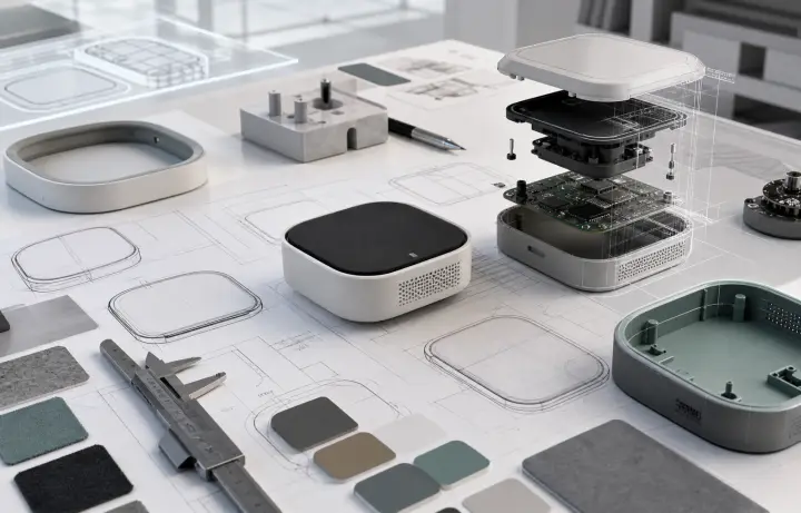
| Challenge | The team had a rough product brief, PCB envelope and target retail positioning, but no manufacturable enclosure direction. | Clarifies why the buyer could not simply approve the next spend. |
| Risk | Exterior styling could easily block ports, vents, antenna clearance, screw bosses or prototype assembly. | Shows the commercial or technical failure mode behind the project. |
| Approach | Align form, internal stack, split lines, vent pattern, fastener strategy and CMF before deeper engineering spend. | Explains how form, structure, prototype route and supplier questions were connected. |
| Evidence package | Product architecture map for PCB, ports, buttons, vents and service access. Exploded enclosure view showing cover, base, PCB, bosses and fastener logic. | Makes the case more credible than a finished image alone. |
| Result | Clarified enclosure direction before full mechanical engineering investment. Reduced avoidable electronics and housing conflicts before prototype spend. | Helps similar buyers judge whether the same path fits their product stage. |
The buyer should be able to inspect more than a finished image: inputs, structure, prototype notes and production risks all matter.
Target user, use case, constraints, open questions and success criteria.
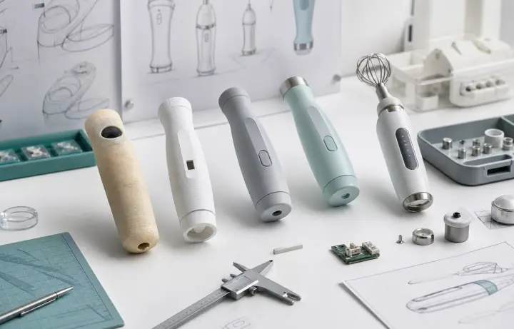
Structure, assembly intent, dimensions, exploded views and supplier-ready references.
Sample method, inspection points, revision path and what the prototype must prove.
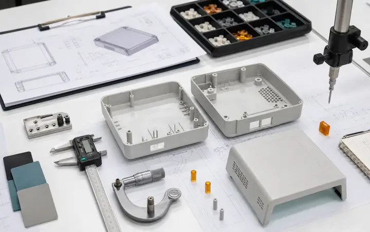
Wall, draft, material, tooling, supplier feedback and pilot approval notes.
A useful case explains the decision path, not only the final visual.
The team had a rough product brief, PCB envelope and target retail positioning, but no manufacturable enclosure direction.
Exterior styling could easily block ports, vents, antenna clearance, screw bosses or prototype assembly.
Align form, internal stack, split lines, vent pattern, fastener strategy and CMF before deeper engineering spend.
V2 case pages separate inputs, evidence and approval gate so buyers can judge whether a similar engagement fits their stage.
Product goal, current files, target user, constraints, references and supplier or prototype context when available.
Form, structure, 3D files, prototype, DFM or supplier-review artifacts tied to the decision being made.
A practical next decision: fund engineering files, build prototype, revise before tooling, ask supplier questions or approve pilot conditions.
A premium industrial design case needs visual and technical proof across form, structure, prototype and manufacturing risk.
These anonymized outputs show the kind of evidence buyers should expect.
The first review gets faster when the buyer can share the few details that define the next risk.